Contents
Why this project was made
As a student of the undergraduate program in Industrial Automation and Robotics, I also had a PLC programming course. Although it wasn't required to make a sophisticated project, I wanted to provide a quality project with custom graphics and something which could have been a real industrial process. At the time of conceptualization I was impressed by PCB design — I even designed my own PCB in Altium Designer because I was in a student circle at the time.
Although I knew the topic is wide enough to fill a PhD thesis, I decided to go for it. After many hours of debugging, researching, and looking for components, I eventually shipped the final version of the project.
What I learned:
- PLC programming in CodeSYS environment with the following languages: SFC (Sequential Function Chart), ST (Structured Text), LD (Ladder Diagram)
- HMI prototype design — designing an operator interface covering normal operation, fault states, service mode, and real-time visualization of machine state
- The PCB assembly production ecosystem — understanding how a real SMT line is structured, what each station does, and how products flow through it
- Soldering techniques: THT (Through-Hole Technology), SMT (Surface-Mount Technology), BGA (Ball Grid Array)
- Types of soldering faults and their causes, with special emphasis on SMT
- Reflow soldering thermal profile
- Improved drawing of electrical schematics in EPLAN Electric P8
- Preparing BOM lists — researching and selecting real, purchasable parts (sensors, actuators, conveyors, PLCs) from manufacturer catalogs and distributor listings
Introduction to PCBs and soldering
What are PCBs and why do we solder?
PCBs (Printed Circuit Boards) are the backbone of every modern electronic device — from smartphones and laptops to industrial controllers and medical equipment. Before PCBs existed, electronic circuits were built by hand-wiring individual components together, a process that was slow, expensive, and nearly impossible to reproduce consistently at scale.
A PCB solves this by replacing physical wires with copper traces etched directly into the board, creating electrical connections that are compact, reliable, and — importantly — identical across every unit manufactured from the same design. Modern boards can have multiple layers of these copper traces stacked inside a single board, allowing extraordinary complexity in a very small footprint. Soldering is what physically and electrically attaches components to the PCB. A good solder joint does two things simultaneously: it creates a reliable electrical connection between the component and the copper pad, and it mechanically locks the component in place so it can withstand vibration, thermal cycling, and everyday handling.
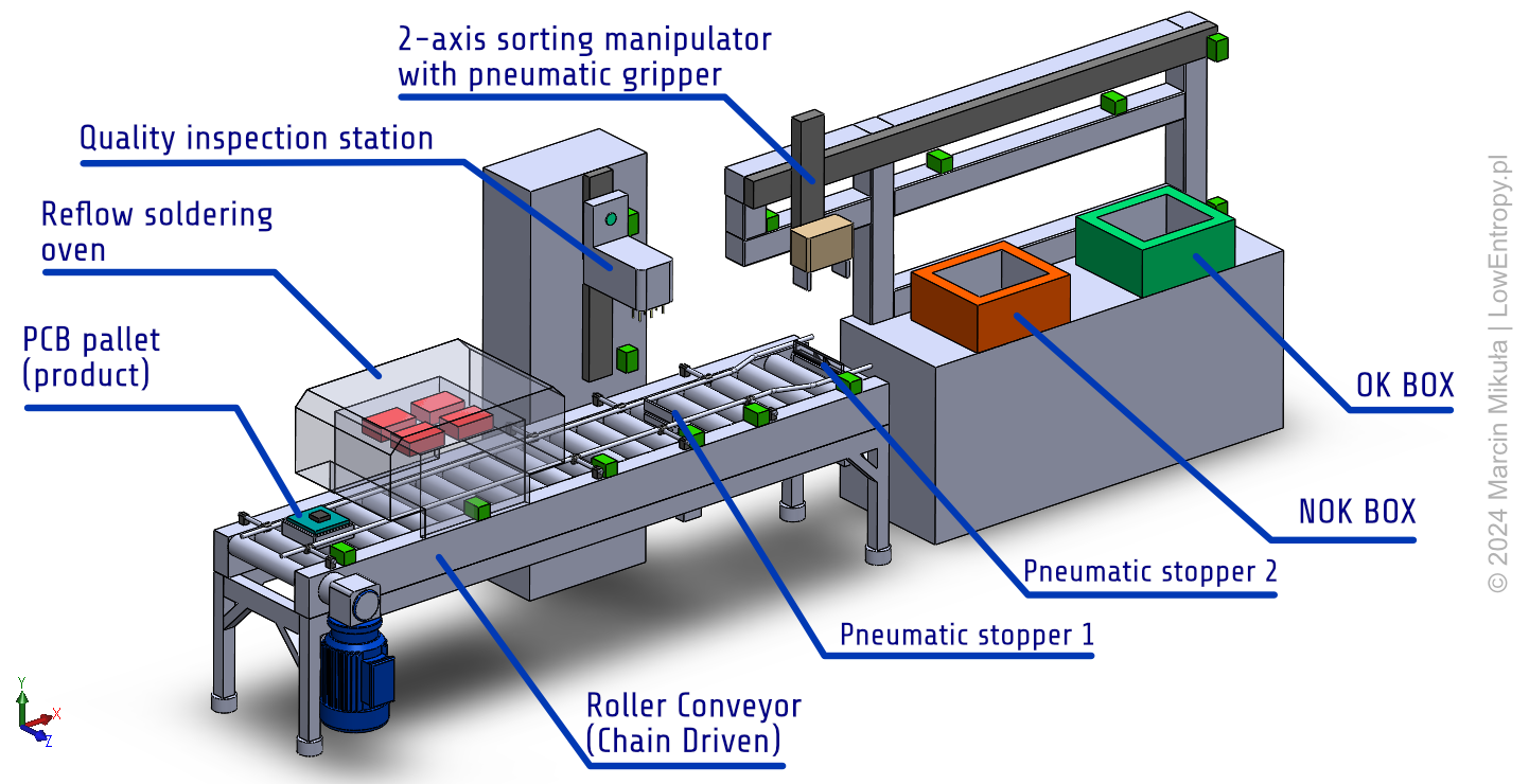
Isometric view of a simplified PCB SMT assembly line model.
Soldering techniques
There are several soldering techniques used in electronics manufacturing, each suited to a different component type or production requirement. The three most widely known are Through-Hole Technology (THT), Surface-Mount Technology (SMT), and Ball Grid Array (BGA) soldering — ranging from the oldest and most manual-friendly to the most dense and automated.
Through-Hole Technology (THT)
In Through-Hole Technology, component leads are inserted through drilled holes in the PCB and soldered on the opposite side, forming a strong mechanical and electrical bond. THT is the oldest of the three techniques and remains common today for components that must withstand significant mechanical stress — such as large capacitors, connectors, and transformers — because the lead going through the board provides a much stronger physical anchor than a surface-mounted joint. The downside is that drilling holes adds cost, components take up space on both sides of the board, and the process is harder to fully automate compared to SMT.
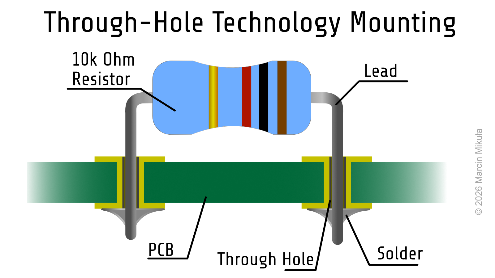
Through-hole components with leads inserted through drilled holes and soldered on the reverse side.
Surface-Mount Technology (SMT)
In Surface-Mount Technology, components are mounted directly onto the surface of the PCB without any drilled holes. Instead of leads going through the board, SMD (Surface-Mount Device) components have metallic termination caps that sit on top of copper pads, bonded by a solder joint on each side. SMT is the dominant technique in modern electronics manufacturing because it enables much higher component density, smaller board sizes, and full process automation — a single pick-and-place machine can place thousands of components per hour with sub-millimeter precision.
The SMT assembly process follows three key steps: first, solder paste — a mixture of tiny solder particles suspended in flux — is applied to the pads through a metal stencil. Then components are placed onto the paste, which holds them temporarily in position. Finally, the board passes through a reflow oven, where a precisely controlled temperature profile melts the paste and forms permanent solder joints. The shape and quality of those joints is exactly what standards like IPC-A-610 are designed to evaluate.
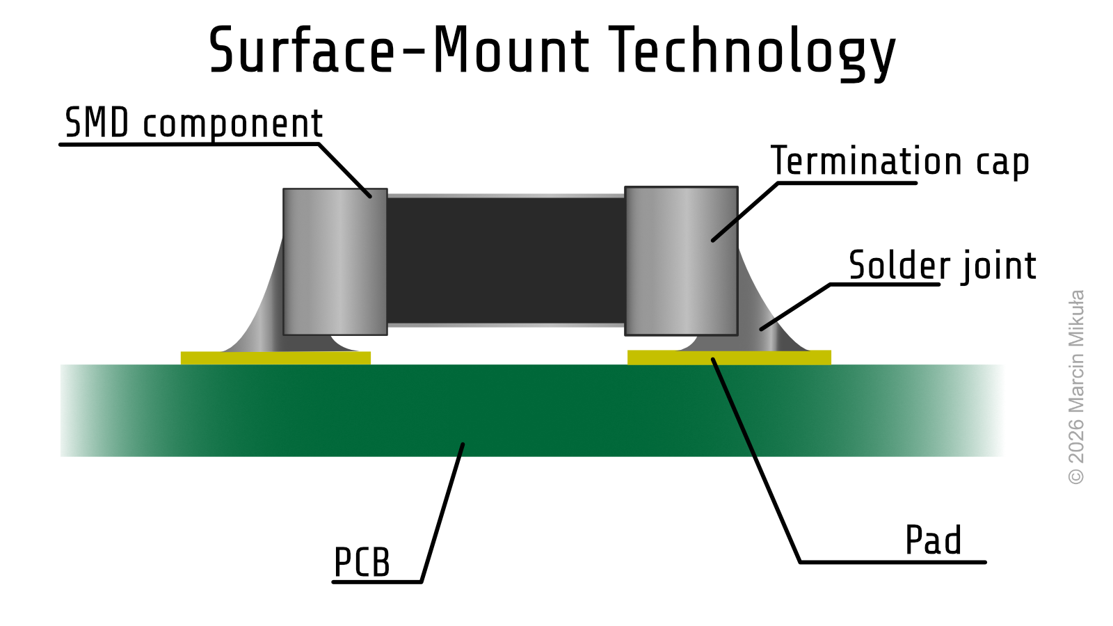
Surface-mount components placed on copper pads before reflow — no drilled holes required.
Common SMT soldering failures
SMT soldering is a precise process — and small deviations in temperature, paste quality, or pad design can cause serious defects. The most common ones are:
- Tombstoning — one end of the component lifts off the pad during reflow, standing it upright like a tombstone. Caused by uneven heating of the two pads.
- Cold solder joint — the solder didn't fully melt or cooled too fast, leaving a dull, grainy joint that looks wrong and is mechanically weak. There may be no electrical connection at all.
- Solder balling — tiny stray solder spheres form on the board surface, usually from moisture in the paste or a misaligned stencil. Can cause shorts if they land between conductors.
- Solder bridging — solder flows between two adjacent pads creating an unintended short circuit. Usually caused by too much paste or a dirty stencil.
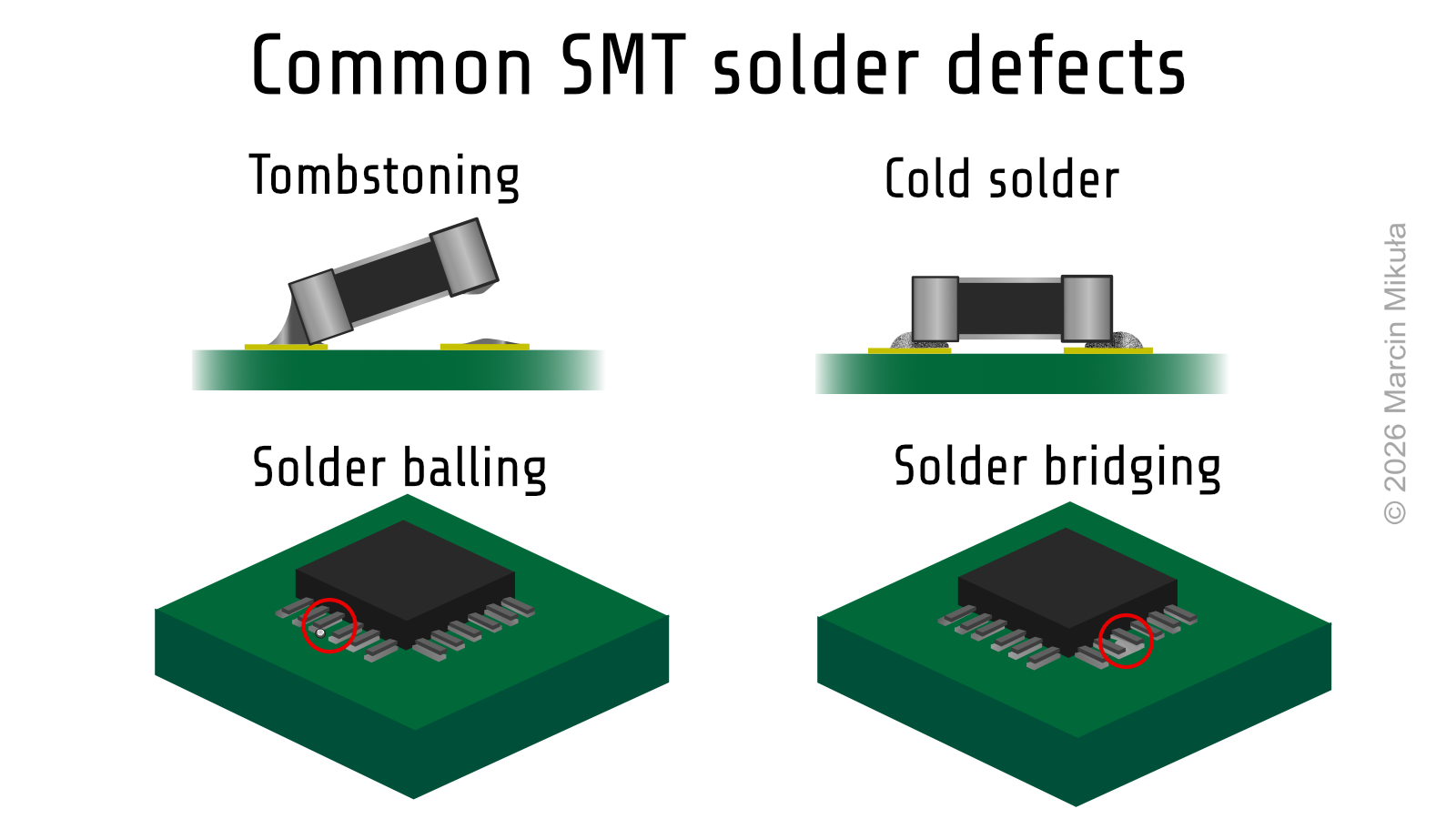
Typical SMT defects: tombstoning, cold joints, solder bridging, and solder balling.
The Reflow Soldering Thermal Profile
The reflow oven follows a carefully shaped temperature curve — critical to joint quality. The profile moves through several distinct stages:
- Ramp to Soak — the board heats gradually to 150–180°C. Solvents in the solder paste evaporate and the flux activates. Heating too fast causes thermal shock to components.
- Preheat / Soak Zone — temperature holds steady for 60–120 seconds, allowing the entire board to reach a uniform temperature and the solder paste to prepare for melting.
- Ramp to Peak / Reflow Zone — temperature climbs to 220–260°C, crossing the solder paste's liquidus point and forming the actual joints. The time spent above liquidus is a critical parameter — ideally 20 to 40 seconds. Too short and the paste doesn't fully melt, leaving poorly formed joints. Too long and components risk overheating.
- Cooling Zone — the board cools at a controlled rate of 2–4°C per second. Cooling too fast introduces thermal stress that can crack the joints.
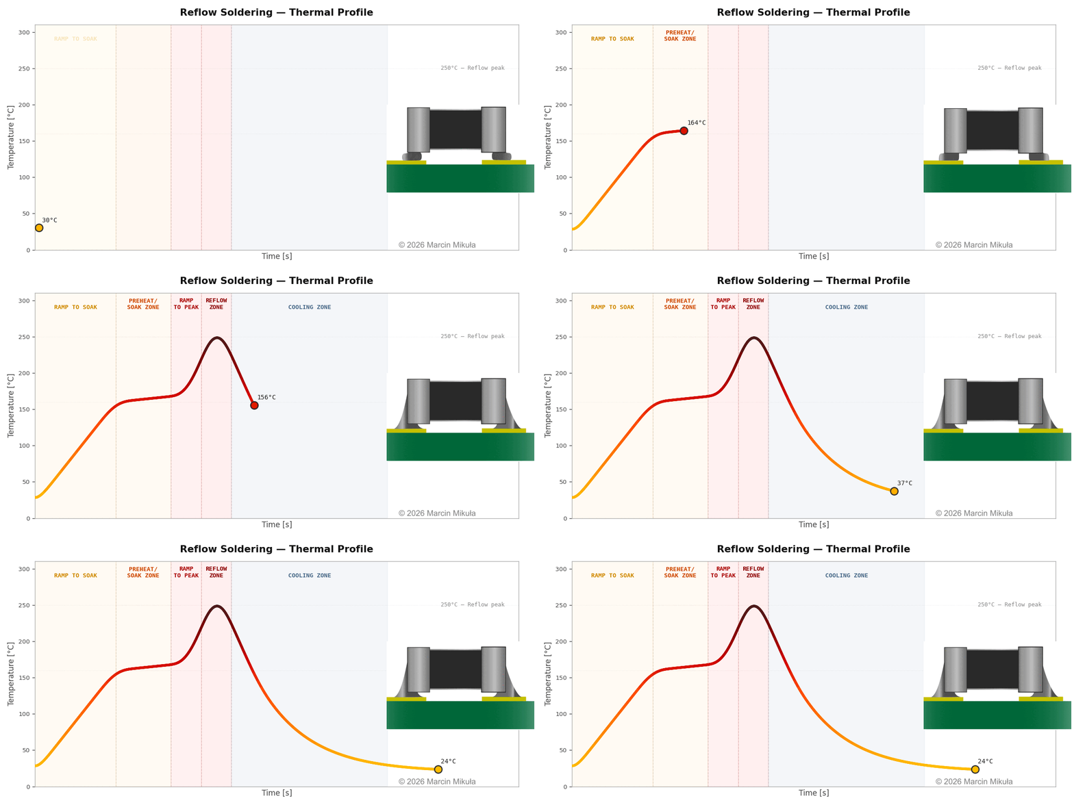
Animated reflow soldering thermal profile — ramp, soak, reflow peak, and controlled cooling.
References
- Altium Education — Fascinating Course about PCBs
- IPC-A-610J: Acceptability of Electronic Assemblies. IPC — Association Connecting Electronics Industries, 2024. Available at shop.electronics.org
- Panasonic — Temperature Profile for Connector Reflow Mounting
- AllPCB — SMT Reflow Soldering Profile